|
|
|
Research Themes (Selected)
1. Advanced Technology Development for Micro/Nanoscale Thermal Probing and Characterization The long-term goal is to understand and control the energy transport at the micro/nanoscale that is involved in nanomanufacturing, material design, structure tailoring, renewable energy application, and material synthesis. Thermal diffusivity, thermal conductivity, specific heat, and interface thermal contact resistance are some of the most critical properties used for thermal design, material/device performance evaluation, and energy conversion efficiency evaluation (thermoelectric, pyrolysis, and thermogalvanic). When the material size goes down to micro and nanoscale, precise measurement of these properties become extremely challenging and difficult. We have invented various advanced techniques to overcome this challenge and conducted unprecedented study of energy transport down to sub-nm level. [Details]
2. Transport phenomena down to Sub-nm Scale : Effect of Material Structure This is a very broad topic, evidenced by a significant number of scholars working in this area world-wide. Our work has been focused on those related to novel material design and structure tailoring, thermoelectric energy conversion, nanoelectronics performance and design. Our studied transport phenomena include phonons, electrons, and charge carrier (hot carrier). Both experiment and atomistic modeling are being carried out in our lab. Some of our findings/discoveries include the pioneering exploration of the coherent lattice interface in thermoelectric materials, electron tunneling and hopping by organic substrates, and extremely confined electron scattering down to 3-atom thickness, and hot carrier transport/diffusion in 2D materials. The research is conducted toward nanomanufacturing with optimal quality control, well-defined material property tailoring, new material discovery, mechanisms understanding in energy conversion, and significant efficiency improvement in energy applications. [Details]
3. Sub-wavelength to Nanoscale Thermal, Mechanical, and Optical Physics in Advanced Manufacturing Optical near-field effect has been studied and used widely for advanced nanostructuring (nanopatterning, nanomanufacturing), and for surface structure imaging to break-down the diffraction limit. Our work has pioneered the modeling, probing, and mapping of the near-field induced temperature, stress, and optical fields. This knowledge is of great importance for system design to achieve scalable nanomanufacturing, and for geometry-design to tailor light-structure interaction. [Details]
4. 2D Atomic Layer Energy and Hot Carrier Transport 2D complex structure is promising for a broad array of applications including extremely high resolution sensors and high-performance field-effect transistors. 2D materials' extreme thinness limits its in-plane heat dissipation during device operation. The out-of-plane thermal transport to the adjacent materials plays an important role in heat dissipation for 2D electronics. Extensive computation and novel experimental work are being conducted in our lab to investigate interface energy coupling, hot carrier diffusion, and electron-hole recombination, and explore the effect of local structure and atomic bonds. [Details]
5. Shockwaves in Laser-assisted Manufacturing In pulsed laser-assisted manufacturing, shockwaves could arise when the process is in open-air (non-vacuum). The shockwave will significantly affect the phase explosion, material ablation, plume re-deposition, and solidification. For years, we have been conducting active research to study the formation, inside structure, propagation, and dissipation of shockwaves. The acquired knowledge provides the critical information for quality-control and process design in laser-assisted advanced manufacturing. [Details]
6. Laser-assisted Advanced Manufacturing This is a quite long tradition in our lab for studying various physical behaviors of materials in pulsed laser-assisted manufacturing. Emphasis has been placed on phase explosion, crystallization, defect formation, stress wave formation and propagation, as well as micro/nanoelectronics manufacturing. [Details]
|
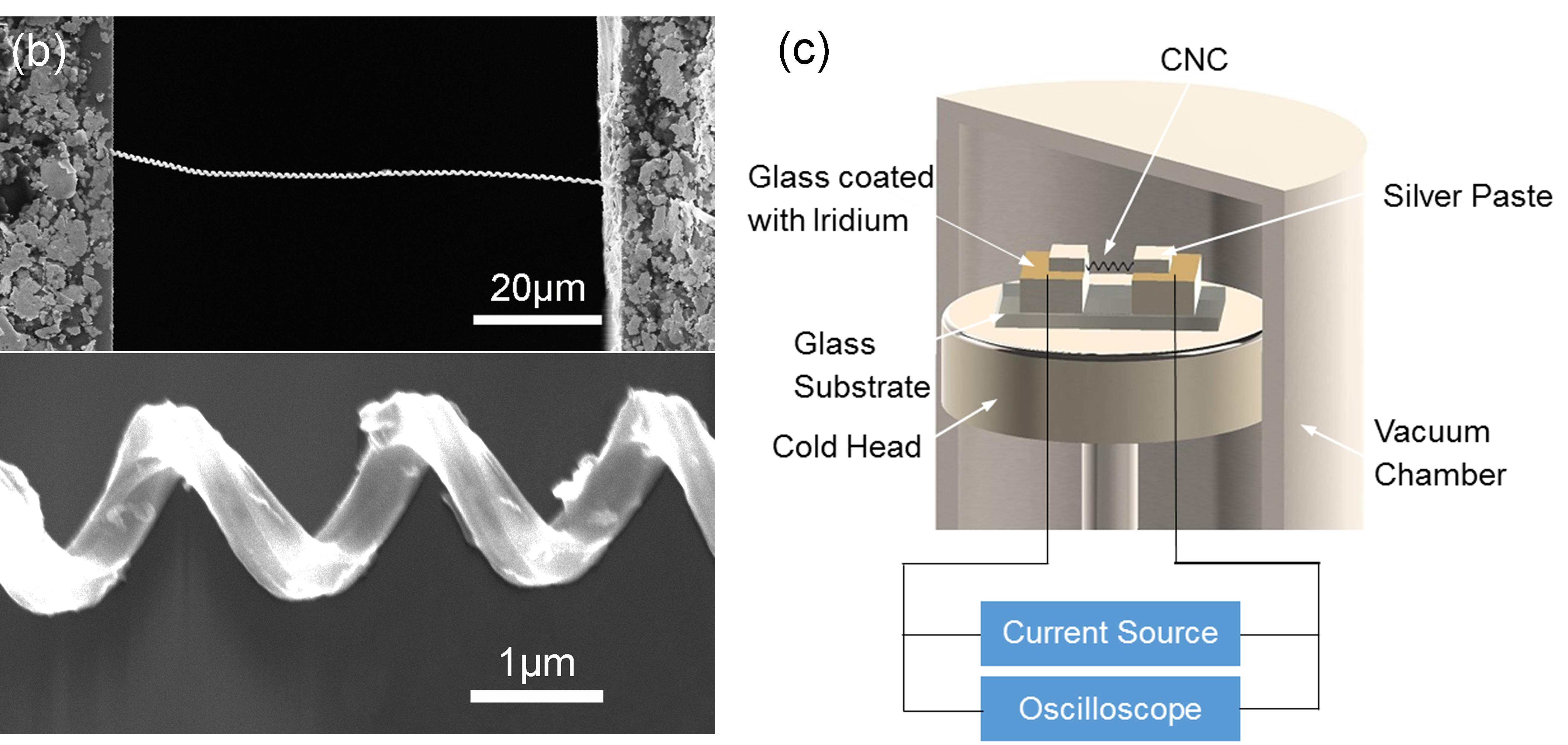
Selected Key Accomplishments 1. Transient Electro-thermal (TET) technique Since our invention of the TET technique in 2007, it almost becomes a golden standard in our lab for measuring the thermal conductivity, thermal diffusivity, and specific heat of fibers and films from sub-mm down to sub-nm thickness. It features great accuracy, ease of conduction, and unprecedented versatility. It is being adopted worldwide for thermal science research at the micro/nanoscale. Representative publication:
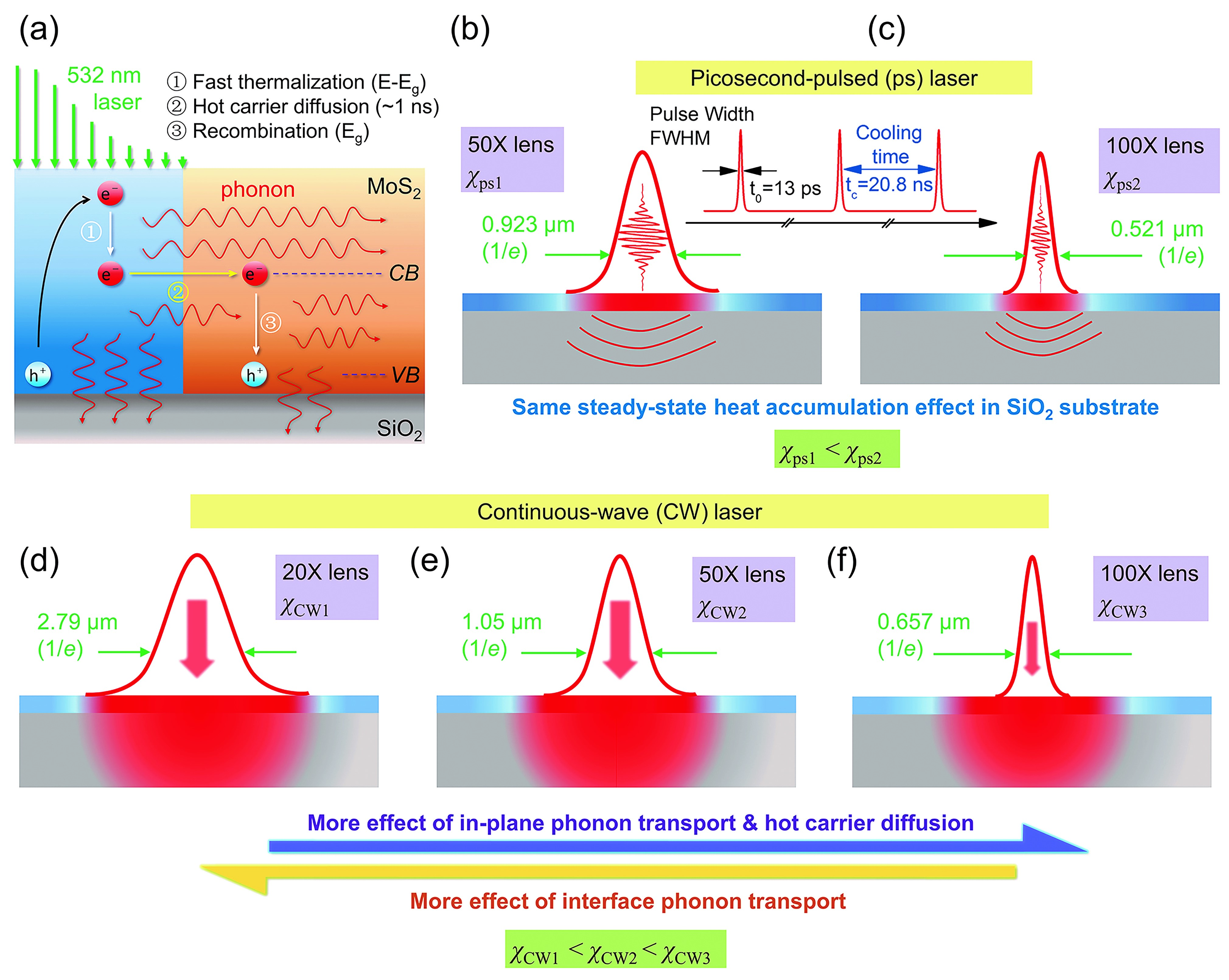
Fig. 1: Carbon nanocoils measured using the TET technique. 2. Energy transport state-resolved Raman (ET-Raman) The ET-Raman technique constructs different energy transport states in space and time domains down to ps, and probes the material's thermal response by measuring the Raman shift power coefficient (RSC). It takes a way completely different from the pump-probe technique in studying a materials' ultrafast thermal response. Also it overcomes some of the critical physical problems faced in steady-state Raman-based techniques for thermal characterization of nanomaterials. It probably represents one of the most advanced Raman-based techniques for characterizing energy transport in nanomaterials. Representative publications: Pengyu Yuan, Ridong Wang, Hong Tan, and Xinwei Wang, 2017, "Energy Transport State Resolved Raman for Probing Interface Energy Transport and Hot Carrier Diffusion in Few-Layered MoS2," ACS Photonics, Vol. 4, pp. 3115-3129 (Supporting Information). Pengyu Yuan, Ridong Wang, Tianyu Wang, Xinwei Wang1, Yangsu Xie, 2018, "Nonmonotonic Thickness-dependence of In-plane Thermal Conductivity of Few-Layered MoS2: 2.4 to 37.8 nm," Physical Chemistry Chemical Physics, 20, 25752. (Supplementary information).
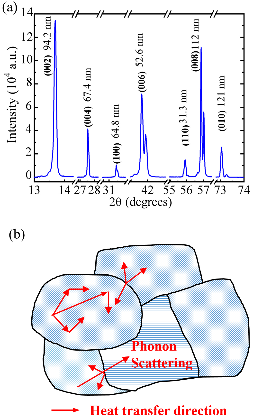
Fig. 2: Schematic of the ps ET-Raman technique for measuring supported 2D materials. 3. Thermal reffusivity The thermal reffusivity theory is constructed and defined to relate a material's electron and phonon transport and scattering with temperature and defect properties. Its variation with temperature directly reflects the structure change and the level of Debye temperature (atomic bonding level). Its residual value at the 0 K-limit reflects the defect scattering of low momentum phonons, and can be used to directly determine a material's structure domain size. This concept has been proved to work extremely well to uncover a structure domain size equivalent and close to that measured by x-ray diffraction. For micro/nanoscale materials and amorphous materials that are hard or impossible to study using beam diffraction, the thermal reffusivity concept still works great in uncovering the structure domain size. Representative publications:
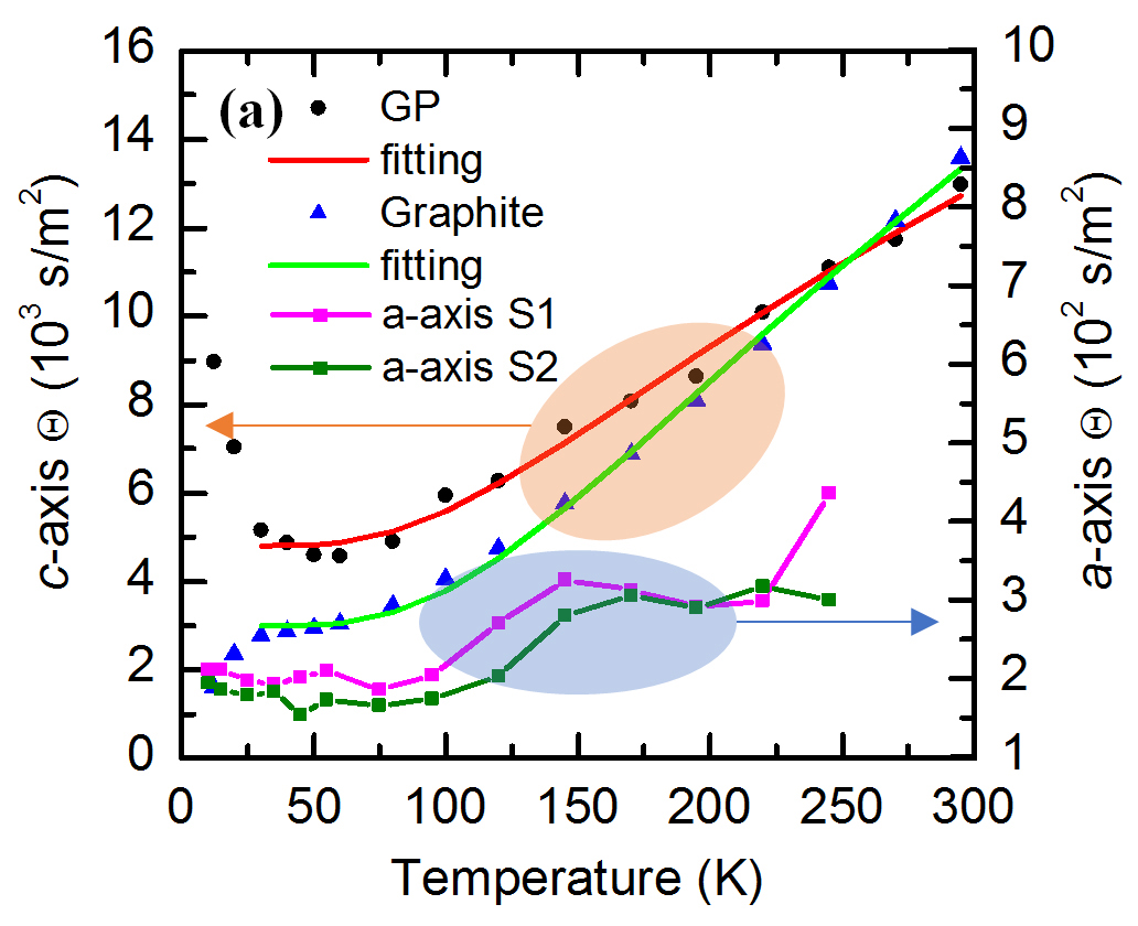
Fig. 3: (a) X-ray diffraction (XRD) of bulk MoSe2 showing the crystallite sizes of 64.8 nm in the (100) direction and 121 nm in the (010)direction. The thermal reffusivity uncovers structure domain size of 58.7 nm and 84.5 nm for 50 nm and 62 nm thick samples, respectively, agreeing very well with the XRD results. (b) Schematic to show the structure domain size defined by thermal reffusivity: it reflects an average crystallite size. 4. Anisotropic specific heat theory This theory is developed to interpret the strong anisotropic heat conduction in 2D materials, especially for the long phonon mean free path in the c-axis. Combined with the thermal reffusivity theory, the structure domain size in the c-axis of 2D materials can be precisely determined with excellent accuracy. Representative publications:
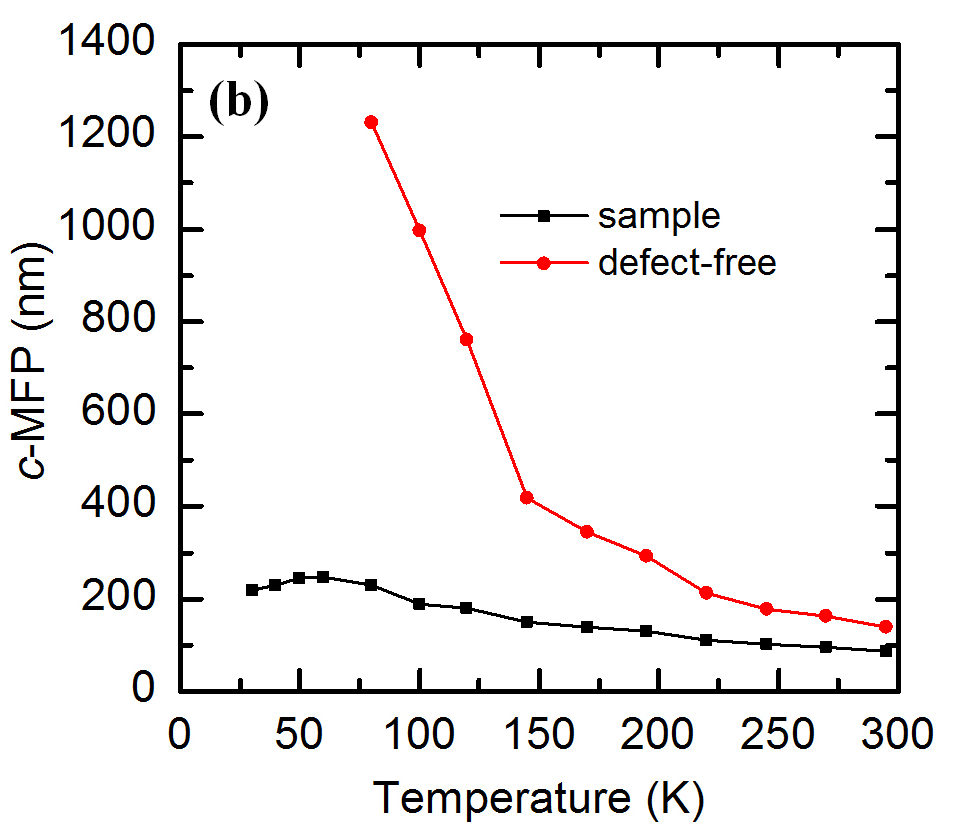
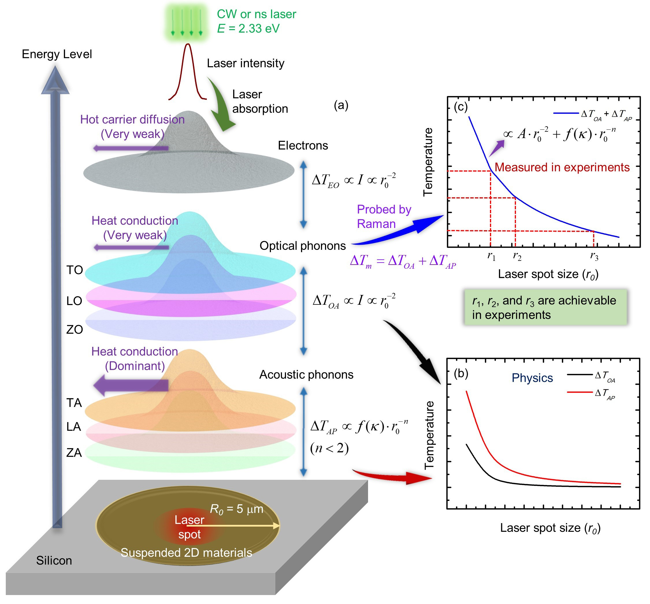
Fig. 4: (a) c-axis thermal reffusivity of graphene paper, and (b) the determined phonon mean free path (MFP) based on the anisotropic specific heat theory. 5. Distinguishing of optical and acoustic phonon temperatures of 2D materials under laser excitation Under photon excitation, 2D materials experience strong cascading energy transfer from electrons to optical phonons (OPs) and acoustic phonons (APs). Despite few modeling works, it remains a long-history open problem to distinguish the OP and AP temperatures, not to mention characterizing their energy coupling factor (G). For the first time, we have designed novel experiments to distinguish the temperatures of OPs and APs, and determine their energy coupling coefficient. Due to the complexity of the problem itself, still significant work is needed in this area, and such study is critical to Raman-based probing of energy transport in nanomaterials. Representative publications: Ridong Wang, Hamidreza Zobeiri, Yangsu Xie, Xinwei Wang, Xing Zhang, Yanan Yue, 2020, "Distinguish Optical and Acoustic Phonon Temperatures and Their Energy Coupling Factor under Photon Excitation in nm 2D Materials," Advanced Science, 2000097 (Supporting information).
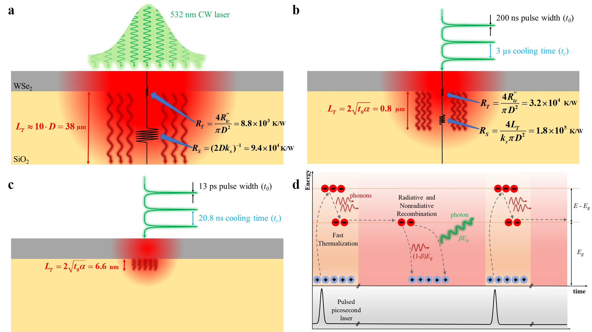
Fig. 5: Physics behind the first distinguishing of optical and acoustic phonon temperatures. 6. Distinguishing of phonon and hot carrier transport in 2D materials In semiconductors, including the extensively studied 2D materials, upon photon excitation, both phonon transport and hot carrier diffusion occur. These two conjugated processes are hard to distinguish and neglecting of the hot carrier diffusion has significantly impeded the understanding of intrinsic phonon transport in these materials. Our lab has designed and conducted first time novel experiments to distinguish the phonon and hot carrier transport, measure the thermal conductivity, hot carrier diffusivity, interface thermal conductance, and determine electron-hole radiative recombination coefficient. This has brought the transport phenomena understanding to an unprecedented level. Also our methodologies open a new non-contact way to characterizing the charge transport in semiconductors. Representative publications: Pengyu Yuan, Ridong Wang, Hong Tan, and Xinwei Wang, 2017, "Energy Transport State Resolved Raman for Probing Interface Energy Transport and Hot Carrier Diffusion in Few-Layered MoS2," ACS Photonics, Vol. 4, pp. 3115-3129 (Supporting Information).
Fig. 6: Distinguishing of hot carrier and phonon transport in monolayer WSe2, and evaluating the radiative electron-hole recombination using ET-Raman.
|
Research Support
Iowa Energy Center Department of Enegy Honeywell Federal Manufacturing & Technologies Army Research Office National Science Foundation California Energy Commission Office of Naval Research Air Force Office of Scientific Research Nebraska Research Initiative Layman Foundation Sumitomo Foundation Nanoconduction, Inc. University of Nebraska-Lincoln Iowa State University
Position Opening To be announced.
.
|

